
Semiconductor Facility Integration
Zero-tolerance environmental control across the manufacturing lifecycle.
The Zero-Tolerance Mandate
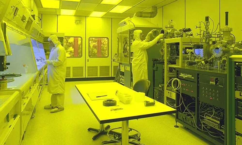
A single fluctuation in temperature, humidity, or particulates destroys a wafer batch.
- Invisible Infrastructure: Continuous environmental stability.
- Precision Control: Automated response to microscopic variances.
Critical Fab Subsystems
Air Handling (MAHU & RCAHU)
Dynamic fan staging balances fresh make-air handling Unit and recirculated cleanroom air handling unit.
Ultrapure Water (UPW)
Real-time TOC, dissolved oxygen, and resistivity loop monitoring.
Front-End Automation

Wafer Prep
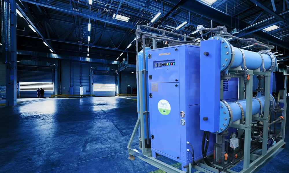
Precision chiller plants and structural vibration monitoring.

FEOL Litho
±0.1°C Sub-Fab HVAC limits and HEPA pressure cascades.

BEOL Metrology
Toxic gas SCADA and real-time exhaust abatement.
Back-End & Assembly Control

Wafer Sort & Test
UPS integration and automated voltage sag prevention.

Assembly Packaging
Strict ESD environment control and energy optimization.
Resilience Architectures

Life Safety & TGM
Automated shutdown and scrubber activation for hazardous gas leaks.

Microgrid Control
Seamless automated switching guarantees 100% critical tool uptime.
Semiconductor / Electronic Manufacturing
| Manufacturing Stage | Process Description | BMS Integration & Control Area |
|---|---|---|
| Wafer Preparation | Slicing raw silicon ingots into ultra-thin, polished wafers. | Vibration & Process Cooling: Monitoring structural vibration and automating precision chiller plants for cutting/polishing equipment. |
| Front-End-of-Line (FEOL) | Transistor formation via photolithography, Etching, Ion Implantation, and Deposition. | Sub-Fab Cleanroom HVAC: Precision temperature (±0.1°C), humidity control, HEPA/ULPA filtration, and strict pressure cascades to prevent particulate contamination. |
| Back-End-of-Line (BEOL) | Metallization; building the microscopic copper/aluminum wiring to connect the transistors. | Chemical & Gas Delivery (SCADA): Real-time monitoring of specialty gas flows, toxic gas leak detection, and automated exhaust abatement. |
| Wafer Sorting & Test | Probing individual dies on the wafer for electrical defects. | Power Quality Management: Uninterruptible Power Supply (UPS) integration and voltage sag monitoring to prevent data loss during continuous testing. |
| Assembly & Packaging | Dicing the wafer, wire bonding, and encapsulating the chips into their final protective housing. | General Facility Control: Standard electrostatic discharge (ESD) environment control, automated lighting, and optimized energy management. |
| High-Speed Diesel Semiconductor and Electronic Manufacturing Units | HSD → Diesel Generator → Electrical Distribution → Critical Manufacturing Loads | Automation Integration & Control: Ensures that HSD is stored, transferred, monitored, and consumed safely and efficiently, while providing operators with real-time information and maintaining accurate fuel accountability. |
Important MSHRIY Role in HSD automation systems
- Automatic Tank Level Monitoring – Continuously measures HSD tank levels and provides high/low-level alarms. (Bulk Storage Tank, Buffer Tank, Day Tank, Overflow Tank)
- Automatic Filling Control – Monitors diesel transfer from the tanker or bulk storage system and prevents overfilling. (Decanting Unit)
- Fuel Flow Metering – Measures the quantity of HSD transferred or consumed.
- Automatic Pump Control – Starts/stops diesel transfer pumps according to tank level or system demand. (Transfer Pump, Pilot Pump)
- Leak Detection – Detects possible fuel leakage from tanks, pipes, or dispensing systems.
- Overfill Protection – Automatically stops filling when the tank reaches its maximum safe level.
- Fuel Dispensing Automation – Controls and records diesel supplied to individual DG sets or equipment.
- DG Fuel Monitoring – Monitors fuel consumption of diesel generators and generates consumption reports.
- Alarm & Emergency Shutdown (ESD) – Provides alarms and automatically shuts down pumps during abnormal or hazardous conditions.
- Redundant PLC/SCADA Integration – Enables operators to monitor tank levels, pump status, flow, alarms, and fuel consumption from a central control system.
- Automatic Mains Failure (AMF) – Detects grid failure and automatically starts the DG and transfers the electrical load when HSD is used for diesel generators.
Semiconductor Wafer Manufacturing
Wafer Preparation
ACTION DESCRIPTION
Ingot slicing, edge grinding, and chemical-mechanical polishing (CMP) to achieve atomic-level surface flatness.
CRITICAL FACILITY CONTROL
Active vibration isolation (<0.5 µm/s) and closed-loop chilled water temperature regulation.
ENVIRONMENTAL SPECIFICATIONS
Lithography & Patterning
ACTION DESCRIPTION
Photoresist spin-coating, deep/extreme UV projection exposure, and chemical pattern development.
CRITICAL FACILITY CONTROL
Ultra-strict environmental control (20.0°C ±0.1°C, 45% ±1% RH) with ULPA air filtration.
ENVIRONMENTAL SPECIFICATIONS
Etching & Doping
ACTION DESCRIPTION
Selective plasma material carving and high-energy ion implantation to alter semiconductor conductivity.
CRITICAL FACILITY CONTROL
Toxic gas exhaust monitoring, acid scrubber abatement, and dedicated chemical drain isolation.
ENVIRONMENTAL SPECIFICATIONS
Metallization & Layering
ACTION DESCRIPTION
Chemical & Physical Vapor Deposition (CVD/PVD) of copper and aluminum micro-interconnect wiring.
CRITICAL FACILITY CONTROL
Specialty gas SCADA delivery systems and continuous Ultra-Pure Water (UPW >18.2 MΩ·cm) supply.
ENVIRONMENTAL SPECIFICATIONS
Test, Dicing & Packaging
ACTION DESCRIPTION
Automated wafer probe testing, precision diamond dicing into individual dies, wire bonding, and encapsulation.
CRITICAL FACILITY CONTROL
Full Electrostatic Discharge (ESD) ionizer shielding and active Uninterruptible Power Supply (UPS) backup.
ENVIRONMENTAL SPECIFICATIONS
End-to-End Semiconductor Manufacturing Process
Ingot Growth & Slicing
Purified molten silicon is crystallized into a massive cylindrical “ingot.” This ingot is sliced using diamond saws into ultra-thin disks called wafers. The wafers are then polished until flawlessly smooth and mirror-like.
Photolithography
A light-sensitive liquid called photoresist is spun onto the wafer. A machine called a stepper projects ultraviolet light through a “mask” (like a stencil) containing the circuit design. The light hardens the exposed photoresist, temporarily printing the circuit pattern onto the silicon.
Etching
The wafer is exposed to liquid chemicals or plasma gases. The areas protected by the hardened photoresist remain untouched, while the unprotected areas are etched away to create 3D microscopic trenches and gates in the silicon. The remaining photoresist is then washed off.
Ion Implantation (Doping)
The wafer is bombarded with beams of charged ions (like boron or phosphorus). These ions embed themselves into specific exposed areas of the silicon, altering its conductivity so it can act as an electrical switch (a transistor).
Deposition and Metallization
Layers of insulating materials and metals (like copper or aluminum) are deposited onto the wafer. Using repeated lithography and etching steps, these metals are patterned into microscopic wires that connect the billions of individual transistors together into a functioning circuit.
Probing, Dicing, and Packaging
Once all layers are built, electronic probes test each individual “die” (chip) on the wafer for defects. The wafer is then cut apart using precision lasers or saws. The working chips are encapsulated in plastic or ceramic packaging, ready to be mounted onto circuit boards.


